



San Francisco Circuits highlights how pogo-pin interfaces can replace permanent programming headers and temporary connectors in compact Printed Circuit Board (PCB) layouts.
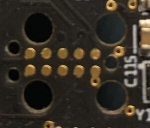
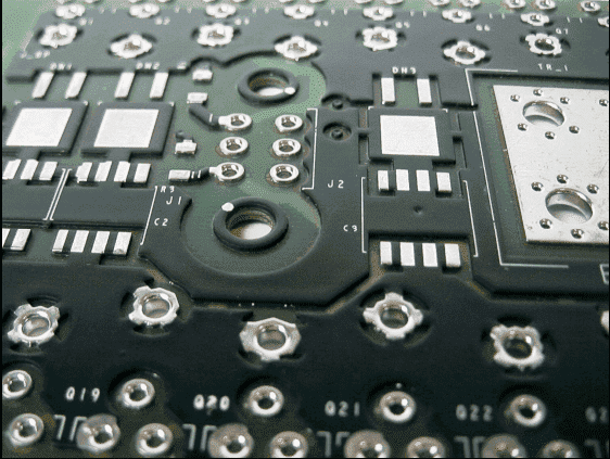
Actual footprint of TC2050 on a Printed Circuit Board
Exposed copper pads paired with spring-loaded contacts maintain access for firmware programming, debugging, and testing while reducing the board area and component cost associated with conventional connectors.
Traditional programming ports can occupy enough space to affect PCB dimensions and, in some applications, the size of the surrounding enclosure. This becomes particularly important in densely populated embedded systems, where processors, BLE modules, WiFi chips, and other programmable devices still require physical access for loading code. Physical connections may also remain necessary during development and debugging, even when remote firmware updates are supported.
Compact Access for Programming and Debugging
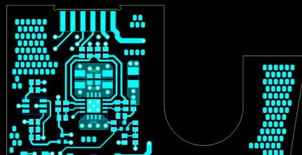
Instead of mounting a programming header permanently, designers can use a small arrangement of exposed copper pads contacted by pogo pins when access is required. This creates a zero-profile interface on the finished PCB while retaining the necessary electrical connections.
Tag-Connect provides this type of solution for JTAG and similar programming interfaces. Its 10-pin legged TC2050 footprint uses additional through-holes for retention clips, allowing the connection to remain secured for hands-free operation. Smaller alignment holes help position the pogo-pin contacts correctly.
Where retention is unnecessary, pogo-pin cables can be held manually during use. More constrained PCB layouts can instead employ legless footprints or trimmed alignment posts when components or mechanical restrictions leave insufficient space for clip holes or other positioning features.
These footprint options allow temporary programming connections to be incorporated into layouts where conventional connectors would be impractical.
Pogo Pins for Testing and Temporary Connections
Programming is not the only application for pogo-pin interfaces. Spring-loaded contacts can also provide access to spare connections, debugging interfaces, and temporary test points that require only occasional access during development or production.
Pogo pins have been used for decades in manufacturing test methods including flying probe systems and bed-of-nails fixtures. These systems can access test pads, exposed vias, and component leads without requiring permanent connectors at each test location.
The same principle can be incorporated into embedded hardware using closely spaced exposed copper pads connected to dedicated test or debug boards. Because these contacts require little PCB area, they can provide access for functional testing and signal probing in space-constrained designs.
Manufacturers including Mill-Max and Harwin offer spring-loaded pin solutions for cable assemblies and PCB integration, providing options for implementing custom pogo-pin interfaces.
Reducing Permanent Hardware on Compact PCBs
For embedded products with limited PCB area, pogo-pin interfaces provide a practical alternative to permanent programming and test connectors. They maintain temporary access for firmware loading, debugging, and testing while avoiding the space, profile, and component cost associated with conventional headers and their mating hardware.
San Francisco Circuits provides PCB manufacturing and assembly expertise for embedded applications, supporting projects from prototype development through production testing strategies.
Read more about pogo-pin based interfaces for saving space on San Francisco Circuits’ website.