


The renewed emphasis on SWAP (Size, Weight + Power) focuses a need for lighter and smaller connectors than older D-Sub solutions. Today’s electronics using COB (chip on board) assembly methods are increasing in density, data acquisition capability and the ability to process high-speed data. New sensors collect signals from multiple sources that are collected and routed to high performance processing chips. IoT and machine-learning systems are feeding data into quantum computing devices to handle multiple functions simultaneously. Neuromorphic computing machines are beginning to mimic the way our brains handle minute signals and compare them to other inputs.
Today’s circuits are also being used in portable devices that require high quality, ruggedized performance. Often times they must perform during or after exposure to high moisture and wide ranges of temperature. New applications require increases in the number of signal lines above the older circuits. Simultaneously, GaAs (Gallium Arsenide), and GaN (Gallium Nitride) chips are increasing signal speeds and are expanding the move to massive digitalization. Multiple lines of data are operating simultaneously at lower voltage and current levels. Designers are demanding smaller sizes, lighter weight, more portability and high-use reliability.
Circuit board design has become a critical skill to ensure on-board circuits support this new era of high-speed digital systems. High-speed circuit board design teams are evolving as specialists. Board designs require matching rise and fall times of each part of the circuit, signal routes are laid out carefully and power distribution is positioned carefully. In some cases, low power noise may have to be filtered on the board itself. Printed line width and spacing on the boards have a key effect on digital speed and performance. The dielectric constant (Dk) of PCB material has become critical in supporting fast rise and fall times of the newer digital signals. Dielectric materials within circuit boards can be polarized and negatively affect speed as well as dissipation factors (Df) of the energy on the surface of the boards themselves. FR-4 materials are being replaced by higher speed substrate materials that reduce the effect of weave and transition losses. Digital signal pairs must also need to be quite similar in length to avoid skew and minimize reflection from one line to the other.
Designers need to add specific attention to connector pads on the printed circuit layout as well. Multiple layout guidelines are well known and required to avoid crosstalk, noise and induced EMI to their signal paths. Correct board design can avoid the effects of noise coupling mechanisms, such as radiation, and magnetic or electric field coupling. Established Micro-D pad layout standards were adopted to help spread-the-distance from pad to pad on the circuit board. This extra distance tended to reduce the “Induced EMI” effect on newer higher-speed digital signals. One example is the Pulse Amplitude Modulation (PAM) signaling set for a NRZ (Non-Return to Zero) method that offers multiple digital lines going through the circuit board and connector. With PAM, each signal uses a “burst” of different voltage levels to isolate each signal from the others. These sudden changes in voltage levels can be noisy, if run to close to other signals on the PCB
When connectors are directly in line with signals on PCBs, “direct coupling” mechanisms, such as impedance, to input/ output signals need to also be considered. The cable-to-connector can become an antenna, adding noise onto one of the signal lines. This noise can then be coupled to the printed circuit board pads and contaminate the signal processing on the boards. Many higher density circuit boards use Micro-D connectors directly in-line with cable.
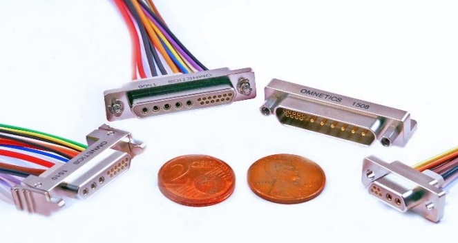
The new circuit applications are used in optical missile seeker heads and phased array controlled radar to autonomous robotics for use in civilian to defense industries. We are now in constant contact with dismounted soldiers who can collect and supply tactical information. Orbital satellites monitor the personal position and health of each soldier in the field. Key circuit modules in those applications are being crammed for space and multi-line interconnection systems from module to module and survive extreme conditions. Additionally, today’s portable test instruments include fully active electronics compared to earlier passive measurement devices. The new portable instruments have evolved in multi-functionality and include additional attachments that collect high levels of data. This requires a significant increase in the number of wires and connectors for the advanced systems. With lower current per signal, wire and connector diameter is reduced to those used in Micro-D connectors. Higher pin counts can now be accommodated in smaller spaces and mount directly to standard patterns on printed circuit boards.
Micro-D connectors have long been a major contributor in the networks of complex systems. More of today’s circuits require less than one ampere of current for multiple signals running at less than 15 volts. Chips are mounted directly on printed circuit boards and are crammed into tight spaces and/or out at the end of a probe or sensor device. The new differential digital signals are fulfilling more needs and run at higher speeds. Single board computers have become the center of larger networks with a complex connector and cable system routing the signals. Information processing and storage occurs at the center of a complex system of data acquisition, data analysis and functional operations.”
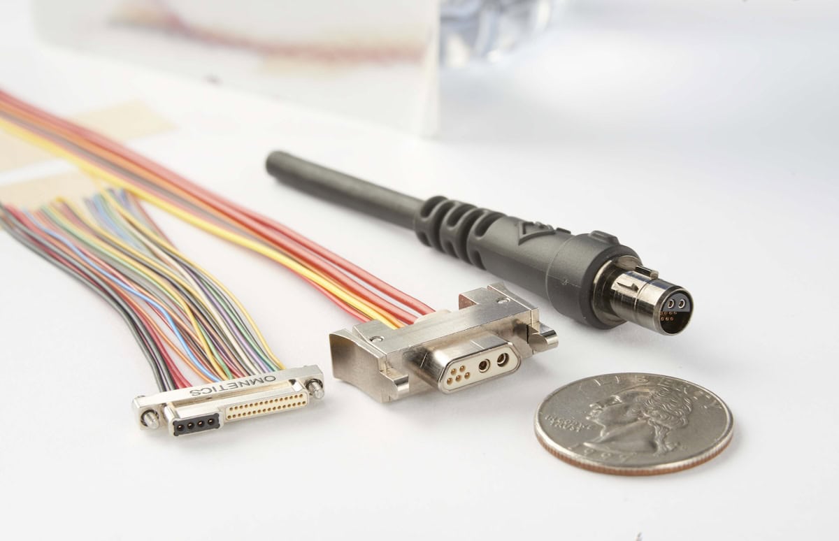
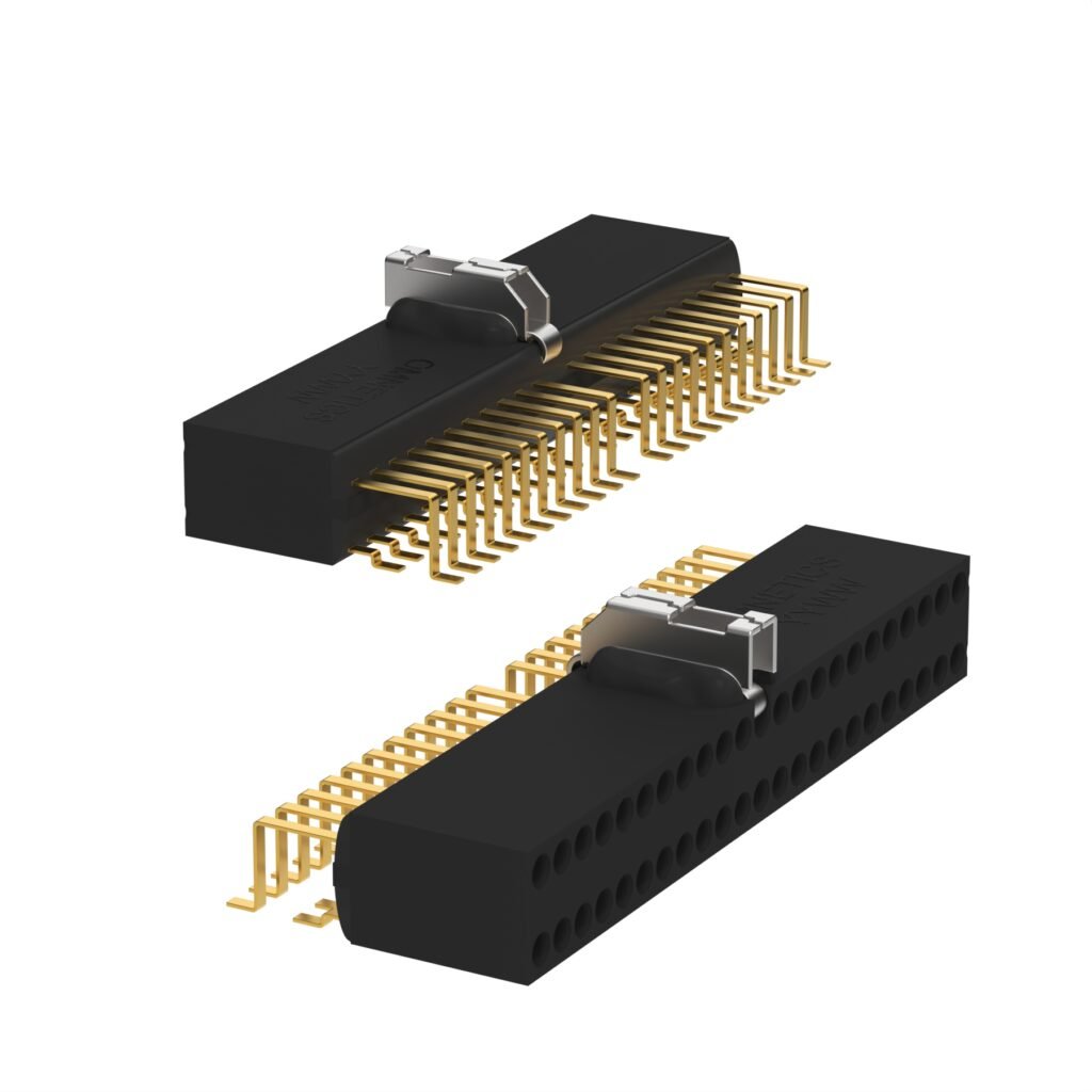
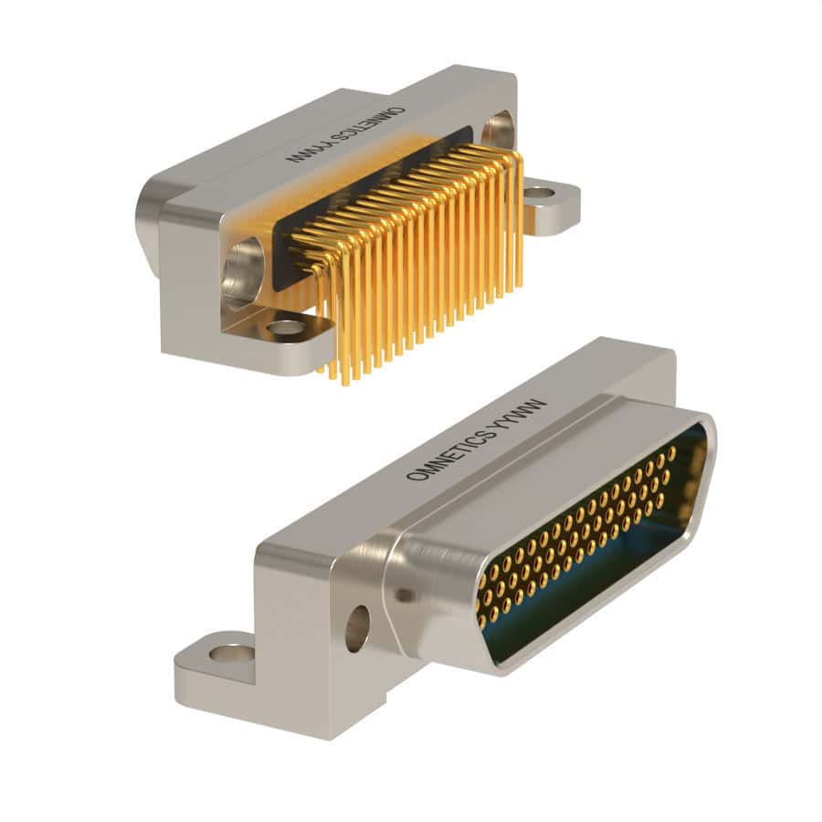
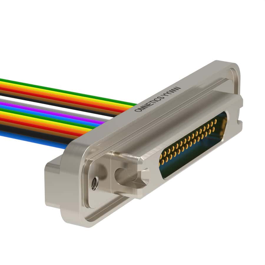
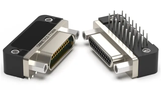
The rectangular Micro-D connectors have matched well with the new chip circuits used for rugged portability, with smaller and lighter weights and pin to pin spacing at .050” centers. The military specification number MIL-DTL-83513 was completed with wire sizes set at 26 AWG to form a standard that handles 3 amperes and lower. The rectangular shape also fits aspect ratios on the printed circuit cards, and can be used as edge connectors as well as assist in higher density stacking of modules. Standard Micro-D with standard circuit board attachment patterns are available in both vertical and right-angle mounting formats and come in a wide range of pin count sizes to from 9 pins to over 37 pins.
Standard mil-spec Micro-Ds fit many applications on most circuit boards in the industry and can be selected on-line. When alternate connector shapes, angles and board mounts are needed, designers can review the standard models and then begin discussions with connector design suppliers to modify those standards to fit well in new instruments. Shell changes to include metal back-shells for EMI shielding and cyber protection are a common example. Mating standard Micro-D connectors is done with jackscrews that require extra time and tools. The newer latching Micro-Ds solve those problems and still hold tightly to work in very rugged applications.
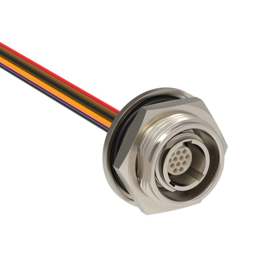
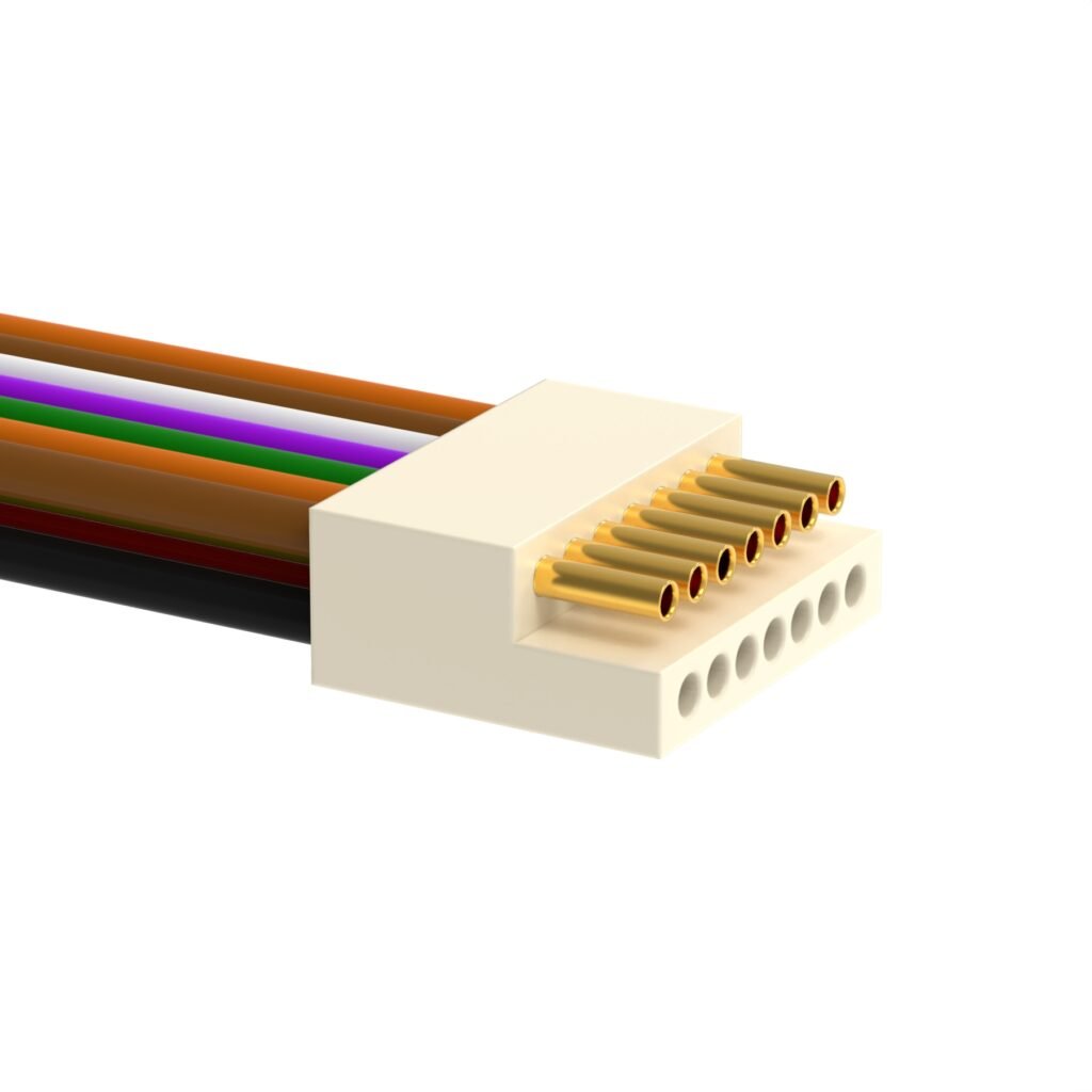
Designers can work directly with Omnetics and others to specify connectors with silicone ring-seals to prevent dust and water ingress. Over-molded polymer covers can bridge the metal connector shell onto the cable jacket providing a smooth transition joint from cable to connector for handling and strain relief. Multiple materials are available, from shells made of aluminum to stainless steel and beyond. Shell plating is selected to match the environmental exposure issues. Back-potting and sealing epoxies are available that can hold above 200˚C or sustain deep space travel with NASA-selected low outgassing.
Higher-speed digital circuits in artificial intelligence, machine learning systems and autonomous robotics are changing the demand for rugged miniaturization. Micro-D connectors can offer a direct match to designs mixing power and signal as well mounting directly onto properly-spaced circuit board patterns that ensure maximum performance of today’s new chip technology. Omnetics uses online solid model work sessions to plan special layouts and offer good variations of connector shapes while simultaneously matching the standard layouts needed on the circuit boards.