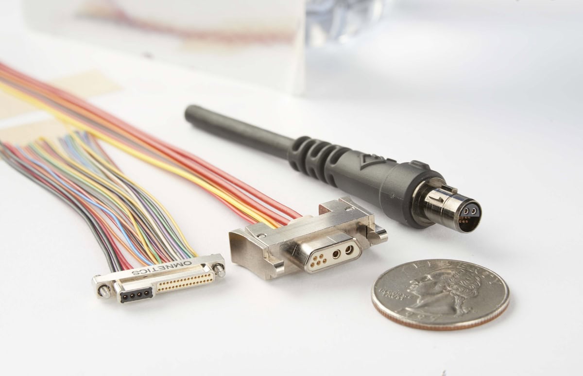


Omnetics has released the following article that discusses how the company’s Micro-D connectors provide a reduced footprint to match amperage and signal path routing throughout miniaturized high-speed system designs, while fitting onto standard printed board layouts.
Careful circuit board layout and signal routing for higher speed digital signal management has become critical. Specific attention to connector pad sizes and patterns on the printed board must be seriously reviewed to support multiple digital signal lines running closely to each other. Layout guidelines are well established to avoid crosstalk, noise and induced EMI to their signal paths.
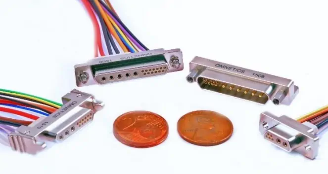
The higher-speed digital signals begin to develop noise and harmonic disturbance effects that can reach to adjacent lines if they are too close to each other. The Omnetics Micro-D standard pad and line spacing is working well for many of the new digital devices and help squeeze more electronics onto the boards than were possible with the larger D-Sub Connectors.
Much of the potential noise transmission, such as radiation and magnetic or electric field coupling, are avoided by using the spacing of Micro-Ds’ standard pads and lines. The pad distance also avoids the “Induced EMI” effect on newer higher speed digital signals, but is not so tight that it causes problems. In addition, board designers must plan for matching rise and fall times of digital signal pathways on their circuit board layouts. Digital signal pairs must also be quite similar in length to avoid skew and minimize reflection from one line to the other.
Careful power source routing and distribution is necessary to avoid low noise coupling and may have to be filtered on the board itself. The dielectric constant (Dk) of PCB materials has become critical in supporting the fast rise and fall times of newer digital signals. Dielectric materials within circuit boards can be polarized during operation and negatively affect speed as well as dissipation factors (DF) of the energy on the surface of the boards themselves. Higher speed substrate materials that reduce the effect of weave and transition losses are also replacing FR-4 materials.
Omnetics Micro-Ds are currently in applications such as optical seeker-heads, ring laser gyros and for board-to-board jumpers in aircraft instrumentation. More portable use of Omnetics connectors include robotic heads and index systems to hand-held weapons and portable communication devices in the military.
A modern example of circuit data digitization using Micro-Ds is being used in support of Pulse Amplitude Modulation, (PAM), signaling, operating at NRZ, (Non-return to Zero) formats. This method depends on multiple digital lines simultaneously going through the circuit board and connector. With PAM, each signal uses a “burst” of different voltage levels to isolate itself from the adjacent signals. These sudden changes in voltage levels can be noisy, if run to close to other signals on the p.c. board. Omnetics Micro-Ds are built to MILDTL-83513 standards and pass performance and rugged testing to meet or exceed those levels.
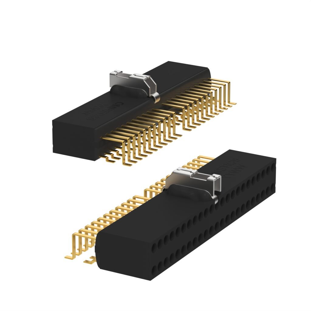
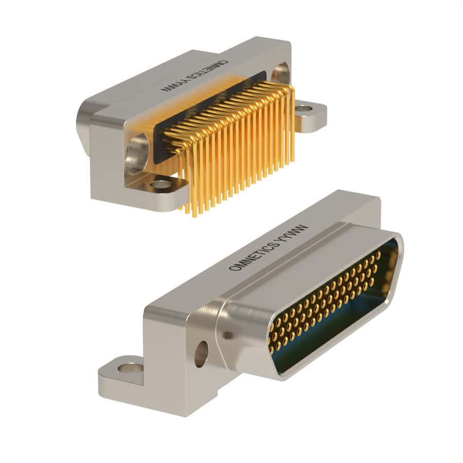
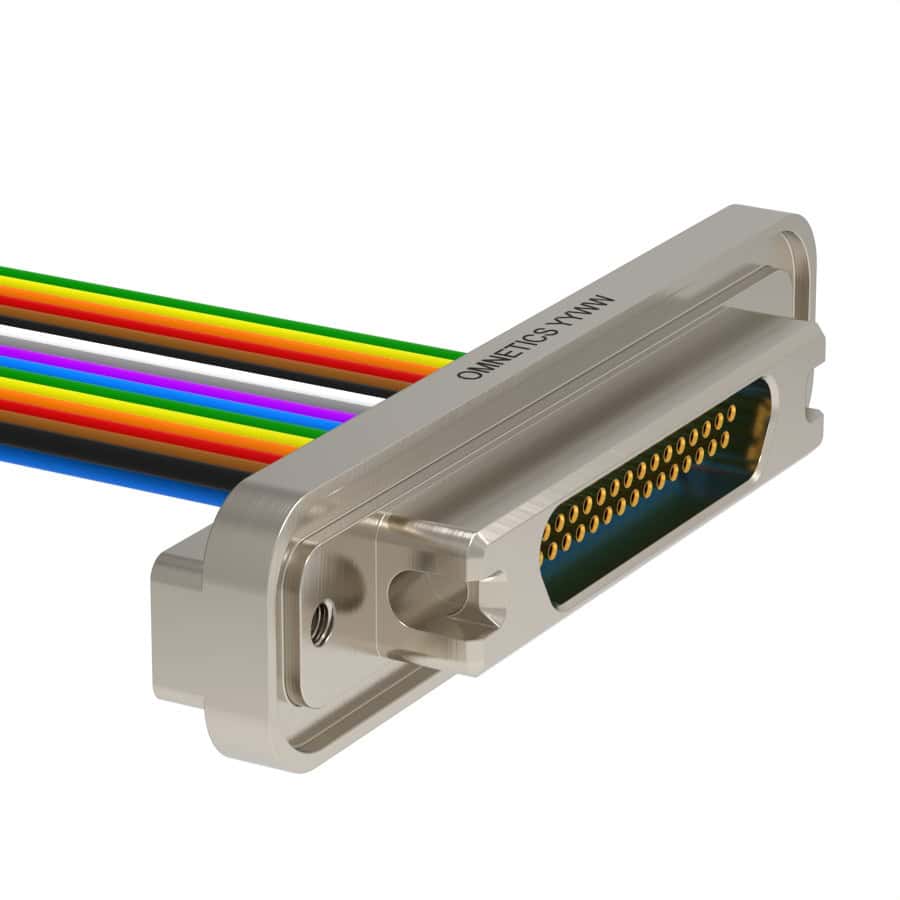
The Standard Micro-Ds fit the approved spacing for mounting on circuit boards and are offered in Vertical Mount as well as Right Angle mounting onto circuit cards. Edge card models are offered and meet with high end wire termination to cable. Approved mating jack-screw lock systems are included that match the military standards. Quick latching shells are also available for applications requiring fast turn over in the field. Omnetics designs exceed shock and vibration specifications and offer continuous low resistance contacts through rugged applications on the battlefield, during weapon launch and in continuous applications such as drone and surveillance devices.
Tailoring Omnetics’ Micro-Ds as needed
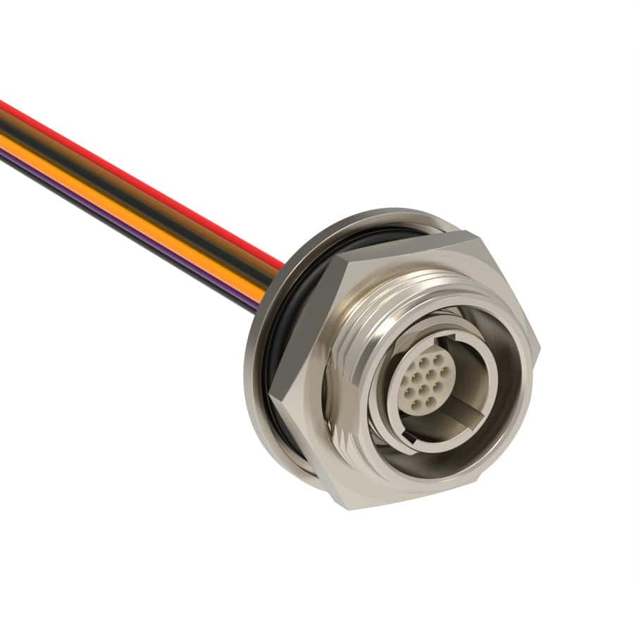
New sizes and shapes are readily adapted from the existing standard designs to meet user applications by modifying our proven products and materials. Multiple materials are ready, from shells made of aluminum to stainless steel and beyond. Shell plating is selected to match the environmental exposure issues and various polymer insulators are available for holding connector pin and sockets in place. Back-potting and sealing epoxies are available that can hold up to 200˚C or sustain deep space travel with NASA-selected low outgassing. For extended strength and highest vibration and shock resistance, the Omnetics Flex Pin was designed from one single piece of BeCu (Beryllium Copper), tempered to 17,200 ksi spring tension. Eliminating the welds and joints in pin design has eliminated potential reliability failures seen in some connectors.
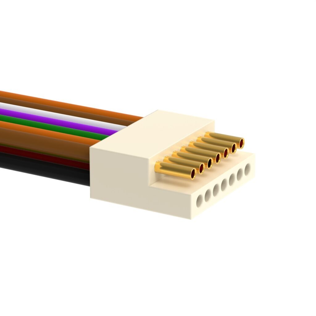
The pin and sockets are pre-formed and subsequently plated with 50 micro inches, (1.27µm) of gold over 50 micro inches, (1.27 µm) of nickel. When selected, the back section of the pins or sockets are formed to insure wire crimping without using solders. Additional back-shells, latching mechanisms and specific shape changes can be done quickly by contacting our Sales Team and or joining our Solid Modeling Designers on-line to configure your unique connector. Options are available from Mixed Signal to Latching connectors and customized back-shells with cable shielding.