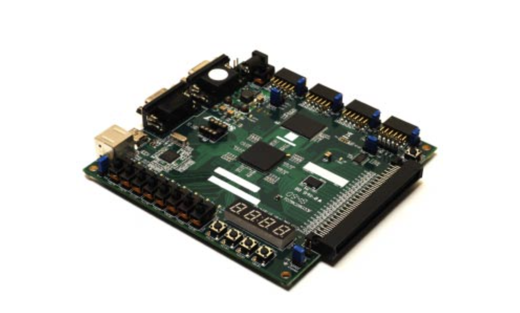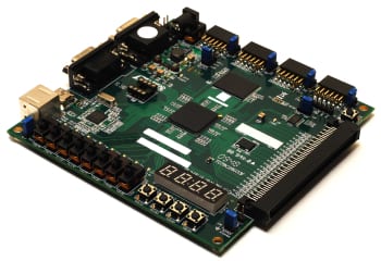


San Francisco Circuits provides PCB fabrication and assembly services, offering both prototype and high-volume production for a range of unmanned system applications.
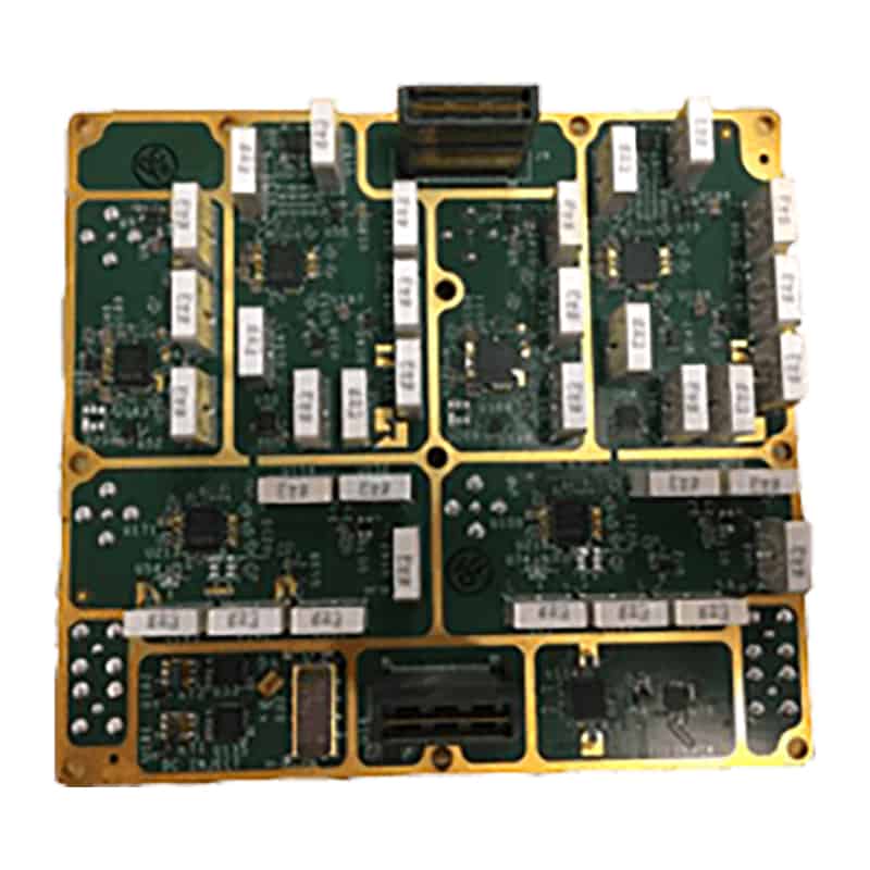
4-layer board containing varying trace widths and types.
Trace width, along with trace length and style, is a key consideration in PCB design and varies based on application-specific requirements.
A PCB trace connects electrical signals—analog, digital, or power—between junctions such as component pins or test points. Trace widths are typically measured in mils (thousandths of an inch).
Trace Width Fundamentals & Design Factors
Standard trace widths for general signals range from 7 to 12 mils, but the specific requirements of a design—such as speed, noise reduction, or current/voltage levels—can drive the need for different trace dimensions. These decisions must be balanced against factors like fabrication cost, board size, and performance.
Certain trace characteristics increase PCB fabrication costs due to tighter tolerances and the need for advanced equipment. These include trace widths and spacing under 5 mils, via holes smaller than 8 mils, non-standard copper thickness, differential pairs, and controlled impedance traces.
High-density designs may require traces as narrow as 2.5 mils and micro-vias as small as 6 mils. High-power applications may need large traces or copper pours across entire layers, while space-constrained designs might use thin boards with half-ounce copper pours.
Performance Considerations for High-Speed & Noise-Sensitive Designs

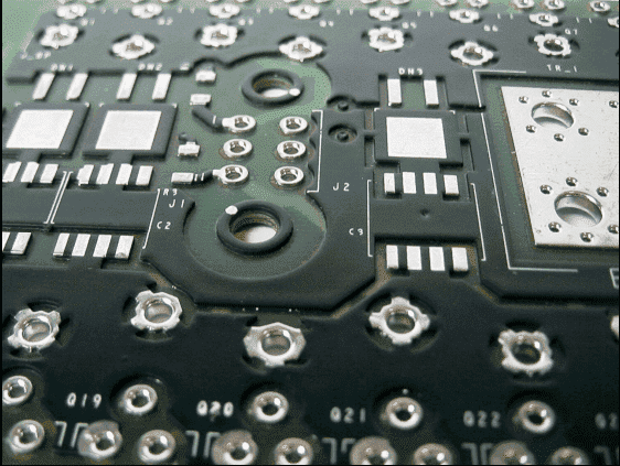
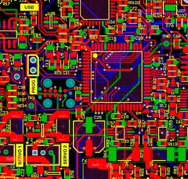
6-layer board containing a 256-pin BGA component with 5-mil trace widths.
Trace width is calculated based on the current the trace must carry. For example, a 2 Amp power trace 0.8 inches long, using 1-ounce copper and operating at room temperature, requires a minimum width of about 30 mils.
This calculation uses IPC guidelines and standard formulas to determine trace area and width. The corresponding voltage drop for this setup is approximately 26mV, which is acceptable for the example application involving a DC motor.
Trace spacing and length are critical for high-speed digital signals. USB 2.0, operating at 480 Mbit/s, requires differential pair routing with matched lengths and 90-Ohm impedance.
A difference in trace length greater than 50 mils can lead to signal reflections. Trace width, spacing, and precise length matching are all necessary to maintain signal integrity. DDR3 memory interfaces are even more tightly constrained and often require software-based trace length tuning.
Noise-sensitive components, such as wireless chips or antennas, benefit from ground-filled traces and planes with embedded vias. These techniques help reduce coupling and protect against off-board noise. Examples include ground-shielded antenna traces and perimeter ground planes on noise-sensitive PCBs.
San Francisco Circuits advises following routing best practices to strike the right balance between fabrication cost, circuit density, and electrical performance. The company supports designs that require complex routing and fabrication beyond standard manufacturing capabilities.