

San Francisco Circuits highlights the critical role of Printed Circuit Board (PCB) stack-ups in ensuring reliability, performance, and cost efficiency. This article explores key considerations, advanced technologies, and best practices to help engineers optimize designs for various applications, from high-frequency RF boards to flexible circuits. Learn more > >

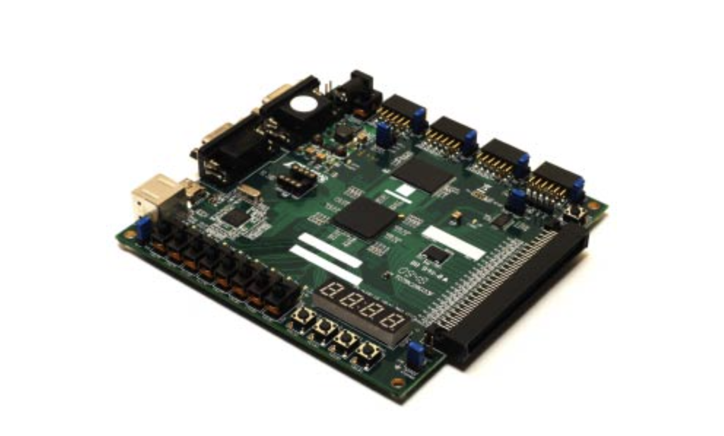
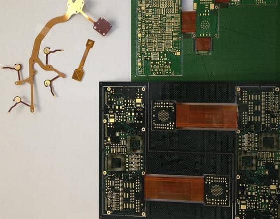
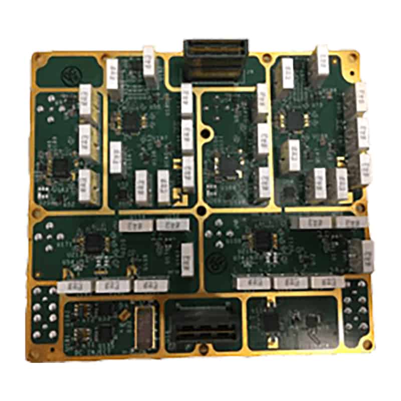
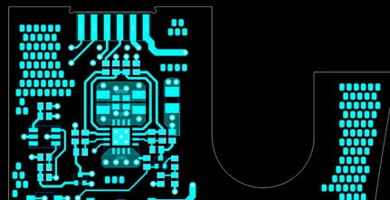
A PCB stack-up outlines the arrangement of copper and insulating layers, influencing signal integrity, power distribution, and electromagnetic interference. Whether working with multi-layer PCBs, metal-core designs, or high-density interconnects (HDIs), each type demands careful consideration. Advanced applications, including high-frequency RF boards and flexible circuits for wearables, have unique stack-up requirements that affect everything from thermal management to mechanical durability.
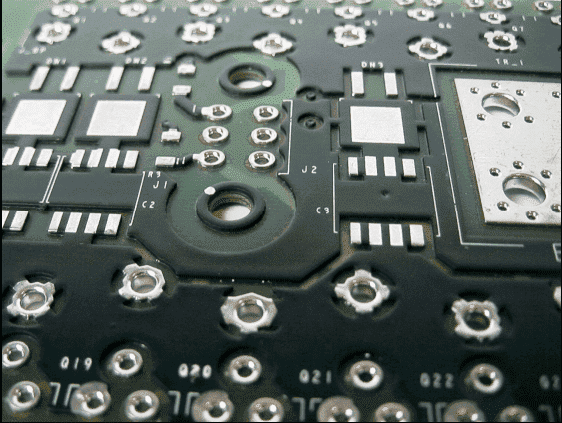
Key factors shaping PCB stack-ups include component density, lamination methods, mechanical constraints, and electrical performance needs. Choosing between foil and cap construction, optimizing ground planes, and ensuring proper impedance control are just a few critical decisions engineers must make.
Understanding these intricacies is crucial to achieving optimal performance and manufacturability.
Read the full article on the San Francisco Circuits website to explore expert insights into PCB stack-ups, best practices, and industry recommendations.