


Read the full article on San Francisco Circuits’ website here
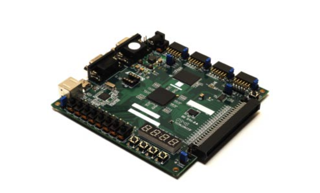
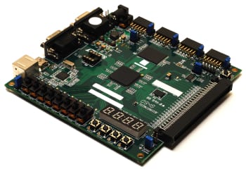
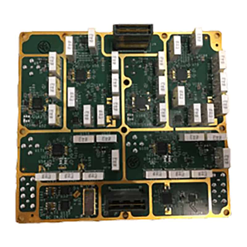
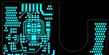
PCB traces connect signals, including analogue, digital and power, from one junction on the board to another. In the case of specific design requirements such as speed optimization, noise or coupling mitigation, or high current/voltage, the implementation of suitable trace widths and types may be more important than optimizing for manufacturing cost of the bare PCB or overall board size.
The article covers:
- What trace width is, and why specifying a particular trace width is important
- Particular trace specifications that can drive up the cost of PCB fabrication and testing
- Examples of various trace widths and thicknesses
- How PCB trace width is calculated
- How PCB trace resistance is calculated
- PCB trace spacing and length
- Ground-filled traces and planes
- Best practices for PCB routing
To find out more about the impact of trace specifications on PCB design, and how to achieve a balance between PCB fabrication cost, circuit density, and overall performance, read the full article on San Francisco Circuits’ website.