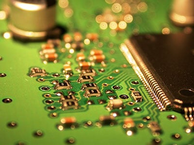


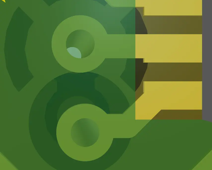
Copper is subject to damage during PCB use or assembly. The soldermask layer applied through via tenting is designed to shield those traces from damage, increase their resistance to overall damage, and help prevent electrical shorts.
Tented vias can also prevent solder from flowing into an untented via hole, which would cause shortages on the PCB’s other side. Though extremely beneficial, via tenting can also cause unique problems. The sealed hole can create a pocket for chemicals, leaving them trapped where they eventually seep into the PCB.
While there are measures that can be taken to prevent that chemical issue, it remains a consideration for designers and assemblers.
If you have more questions about PCB fabrication and assembly, contact San Francisco Circuits’ PCB professionals at 800-SFC-5143 or email [email protected] to ask about your next project.
Read the full article, or visit the company’s website to find out more.