


San Francisco Circuits, a provider of advanced Printed Circuit Board (PCB) fabrication & assembly services, presents examples of rigid PCB stack-ups and how their design affects electrical performance.

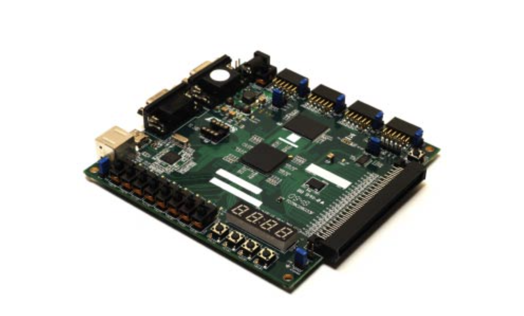
In rigid PCB design, the stack-up determines the thickness and sequence of copper and dielectric layers, directly influencing electrical performance and durability. Copper layers typically range from ½ oz to 2 oz or more, depending on current-handling and signal requirements. The correct configuration ensures optimal routing of power and signals, minimizes interference, and supports thermal stability.
Importance of Precise Stack-Up Definition
Accurate stack-up definition is a critical yet often overlooked stage of PCB design. Incomplete specifications can shift key manufacturing decisions to the fabricator, leading to performance variability. A well-documented stack-up improves reliability, signal integrity, and manufacturability while streamlining coordination between design and production.
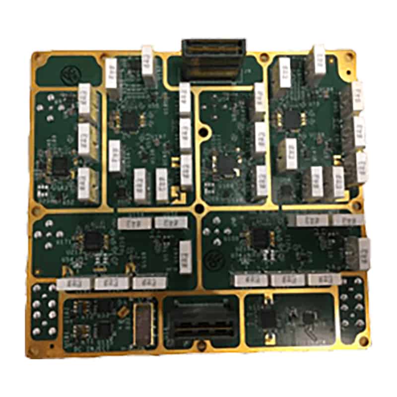
Rigid Stack-Up Examples
Multi-layer rigid PCBs improve signal distribution, reduce cross-interference, and support high-speed data transfer. Their layered structure minimizes external noise, mitigates radiation, and addresses impedance and crosstalk issues, key considerations in high-frequency and mission-critical systems.
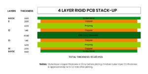
- 4-Layer PCB Stack-Up: Provides enhanced routing capability and improved power distribution while maintaining a compact design.
- 6-Layer Rigid PCB Stack-Up: Used in advanced systems that require dedicated ground and power planes for improved noise isolation and signal fidelity.

Materials and Construction
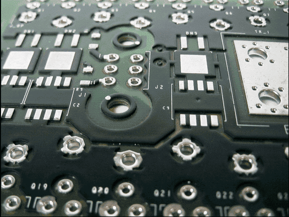
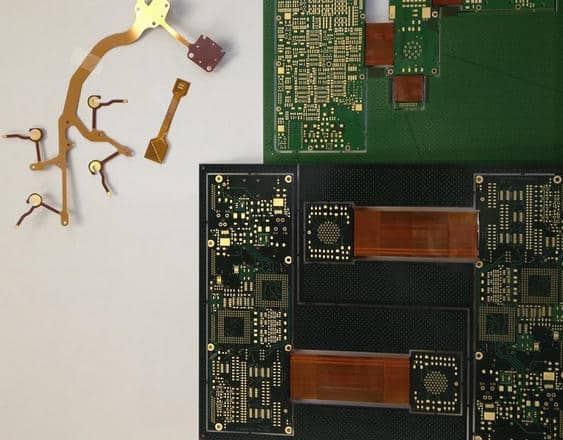
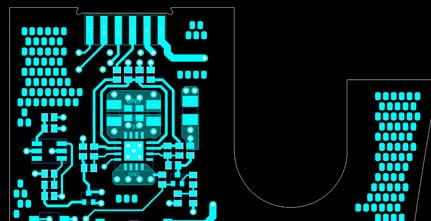
The structure of a stack-up varies according to the PCB’s purpose. Designs intended for hybrid, high-heat, or high-speed applications require tailored materials and dielectric combinations to meet specific electrical and mechanical requirements. A simple single-sided board typically includes a substrate, copper layer, and solder mask, with an optional silkscreen for component labeling. Multi-layer PCBs, by contrast, incorporate multiple copper and dielectric layers joined with prepreg and core materials to form a unified laminate.

There are two main methods of lamination: foil construction and cap construction. Foil construction, the preferred approach, positions prepreg between outer copper layers to improve layer registration, yield, and cost-efficiency. Cap construction, while less common, is used for hybrid PCBs that require specialty laminates or when specific drilling methods, such as laser drilling, are not available.
Design Factors Influencing Stack-Up Requirements
Several factors determine the optimal rigid PCB stack-up configuration:
- Component density: High pin-count BGAs and complex integrated circuits may require additional layers for signal breakout and routing.
- Thermal performance: High-current or power-dense designs use thicker copper planes to manage heat dissipation and maintain electrical stability.
- Signal type: Analog, digital, and high-speed mixed-signal systems demand specific grounding and impedance control to minimize noise and crosstalk.
- Mechanical considerations: Thickness, rigidity, and resistance to vibration or deflection must align with structural and assembly constraints.

Design Tools and Resources
San Francisco Circuits provides an online PCB Stack-Up Calculator Tool, allowing engineers to design and visualize multi-layer configurations from four to fourteen layers. This tool helps balance electrical, thermal, and mechanical factors early in the design process, enabling more predictable manufacturing outcomes.
Find out more from San Francisco Circuits on rigid PCB stack-up configurations.