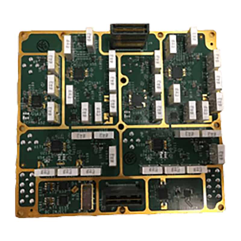


San Francisco Circuits highlights that mastering the different types of Printed Circuit Board (PCB) vias is essential for achieving reliable, space-efficient, and high-performance multilayer board designs.

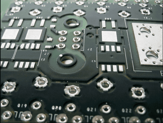
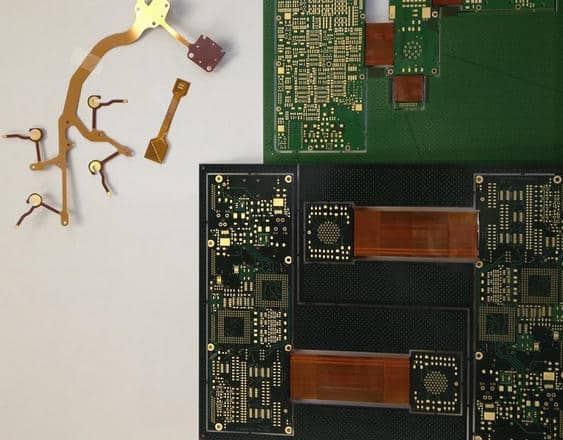
Stacked via from San Francisco Circuits.
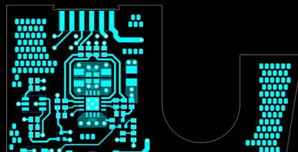
Vias provide the vertical interconnects between copper layers, enabling dense routing and compact architectures across modern electronics.
The most familiar style is the through-hole via, extending from the top to the bottom of the PCB and offering robust mechanical strength. For higher-density layouts, designers rely on blind vias, which link an outer layer to inner layers, and buried vias, which connect only internal layers to preserve critical surface real estate.
Ultra-miniaturized designs frequently incorporate microvias, laser-drilled structures typically ≤150 µm, essential for HDI boards and fine-pitch BGA escape routing. When vertical interconnections must span multiple layers, manufacturers use stacked vias—precisely aligned microvias or blind vias, or staggered vias, which offset each layer transition to enhance reliability and reduce mechanical stress.
To optimize component placement, Via-In-Pad (VIP) technology places vias directly beneath pads, filled and capped to maintain solderability while minimizing signal length. Meanwhile, tented vias, covered with solder mask, help prevent solder wicking and protect against contamination in dense assemblies.
Together, these eight core via types support today’s demands for miniaturization, thermal performance, and high-speed signal integrity. As PCB complexity escalates across defense, aerospace, robotics, and unmanned systems, careful via selection remains fundamental to ensuring manufacturability, reliability, and long-term mission performance.