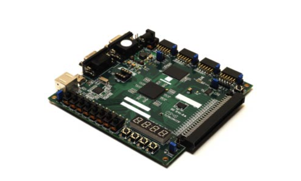


San Francisco Circuits examines insertion loss, a critical factor in Printed Circuit Board (PCB) design that directly impacts signal integrity in high-frequency systems. Read more >>
Insertion loss refers to the reduction in signal strength as it passes through components, cables, or PCB traces, particularly in systems operating above 3 GHz. While some level of loss is unavoidable, understanding its causes allows engineers to develop strategies to minimize its effects and improve overall system performance.
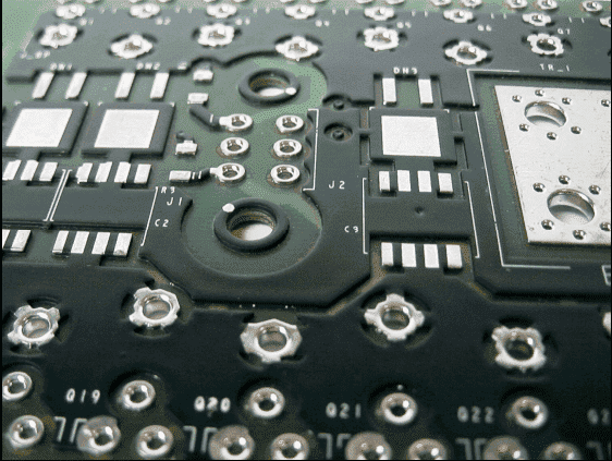
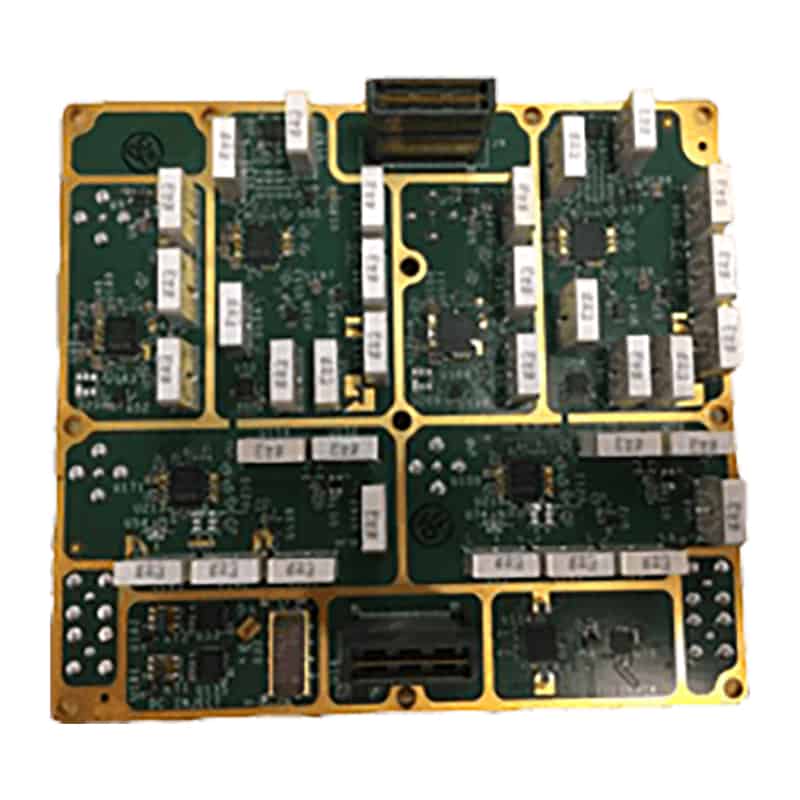
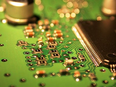
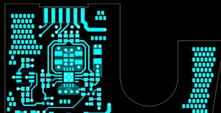
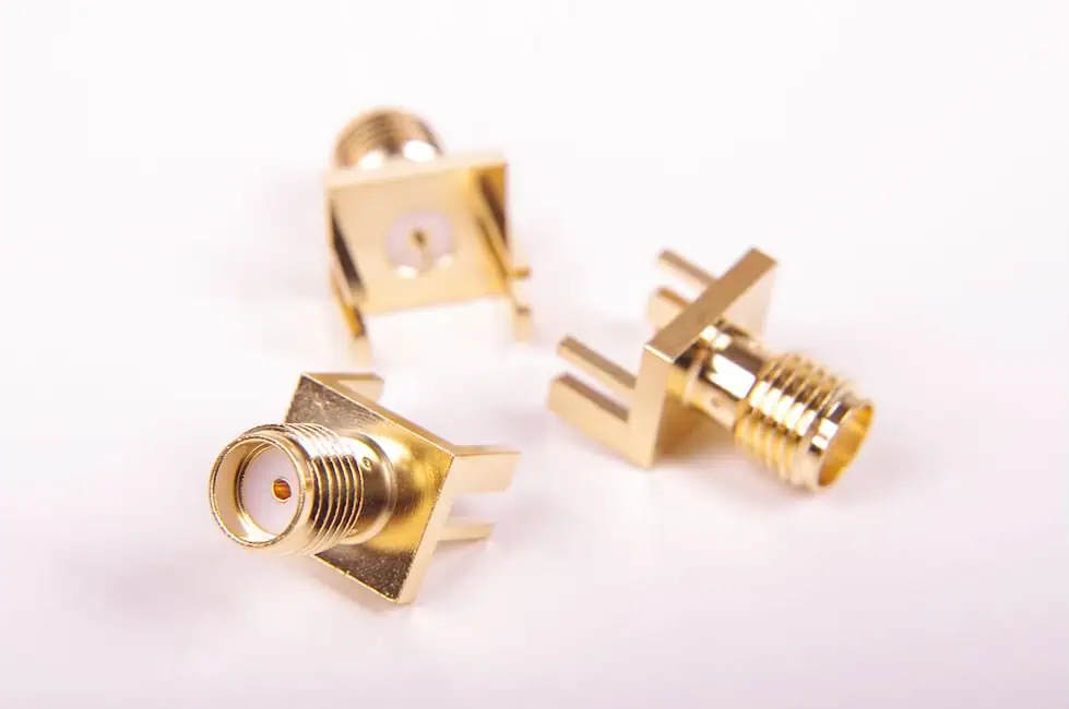
Several contributors play a role in insertion loss, including transmission length, connectors, cabling, material selection, and frequency. Longer transmission paths increase resistance and susceptibility to interference, while poor terminations and impedance mismatches introduce reflections. Connectors and interconnects add further discontinuities, reducing Voltage Standing Wave Ratio (VSWR) and impacting signal quality. PCB materials also play a significant role, with both copper and dielectric losses affecting performance depending on substrate thickness, copper type, and stack-up design.
Insertion loss grows more significant at higher frequencies. In systems above 10 GHz, PCB materials and parasitic effects from vias become dominant contributors. The skin effect, where current concentrates at the conductor’s surface rather than its full cross-section, adds resistance and increases losses. This makes careful material selection and stack-up optimization essential for maintaining signal integrity at higher operating frequencies.
Although insertion loss cannot be eliminated entirely, its impact can be reduced through thoughtful design practices. Shorter transmission paths, optimized connectors, low-loss materials, and precise PCB construction can significantly improve performance. Balancing these technical considerations with production costs is key, and consulting with an experienced provider such as San Francisco Circuits can help engineers make informed trade-offs for reliable, high-speed PCB systems.