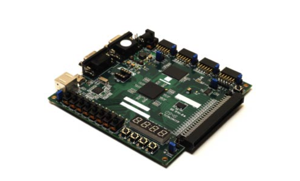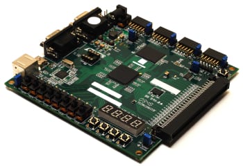


San Francisco Circuits highlights best practices for managing copper pads, traces, and planes in Printed Circuit Boards (PCB) designs for high-load applications. As electronic systems demand higher current and voltage, proper PCB design becomes critical to ensure performance, safety, and reliability. Read more >>

Managing High Current in PCB Design
Copper traces and planes carry electrical current but also introduce resistance, which can lead to voltage drops and heat generation. As trace length increases or width decreases, resistance rises, potentially impacting performance and reliability. Excessive heat can damage components, compromise board integrity, and create safety risks.
To address high current demands, designers can increase trace widths, use heavier copper weights, and distribute current across multiple layers. Techniques such as via stitching help reduce resistance and improve heat dissipation by connecting copper across layers.
Thermal Considerations in High-Load Applications
Thermal management is essential when dealing with high current. PCB stack-up design, material selection, and copper distribution all play a role in heat control. Materials with lower thermal expansion improve durability, while metal core PCBs can help spread heat more effectively.
Additional cooling methods, such as heatsinks and airflow, can further enhance performance. Thermal analysis tools can also be used to identify hotspots and optimize designs before production.
Designing for High Voltage
High-voltage PCB design introduces additional challenges, particularly in maintaining proper spacing between conductive elements. Voltages above 50V can pose safety risks, making it essential to follow industry standards for clearance and creepage distances to prevent arcing.
Designers may also use conformal coatings to add insulation and protection, as well as select advanced substrate materials such as PTFE or polyimide for improved performance under high voltage and temperature conditions.
Testing and Protection Strategies
Ensuring reliability in high-load applications requires robust testing and protection mechanisms. Dielectric (hipot) testing verifies electrical isolation, while protection components such as fuses, current monitors, and surge suppressors help prevent failures.
Incorporating fail-safe features and performing functional testing under load conditions can further reduce risks and improve overall system safety.
San Francisco Circuits – Trusted PCB Partner
San Francisco Circuits provides advanced PCB manufacturing solutions for high-performance applications. From managing copper traces to optimizing designs for high current and voltage, their expertise helps ensure reliable and efficient PCB performance.
Find out more about PCB copper trace design for high-load applications on San Francisco Circuits’ website.