


San Francisco Circuits explores the evolution of microelectronics and PCB production, examining how advances in component packaging, High Density Interconnect (HDI) technology, and fabrication processes continue to support increasingly compact and capable electronic systems. Read more >>

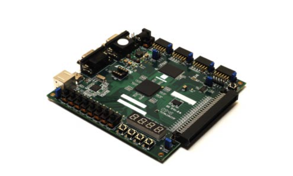
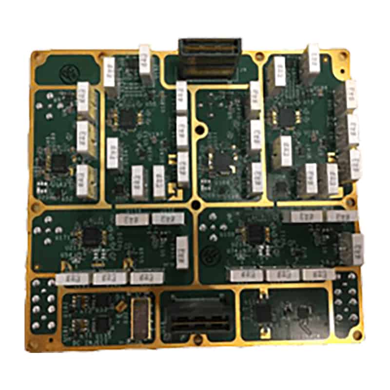
PCIE card with an 802 11n 3×2 MIMO radio.
The company provides PCB manufacturing and assembly solutions for modern microelectronics applications, including HDI fabrication, microvia implementation, prototype development, and production builds.
As electronic devices continue to shrink while delivering greater functionality, PCB designers and manufacturers must adopt new approaches to routing, assembly, and fabrication. Modern microelectronics rely on dense board layouts, advanced component packages, and specialized manufacturing techniques to achieve performance and reliability requirements.
The Shift Toward Higher-Density Components
Earlier PCB designs commonly utilized plated through-hole (PTH) components with larger pin spacing and relatively simple layouts. While these devices simplified routing and assembly, they required more board space and limited overall system density.
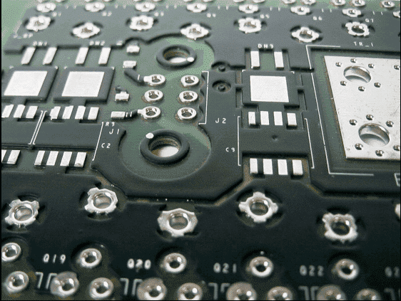
Today, most electronic products utilize surface mount technology (SMT), allowing significantly greater component density and improved electrical performance. Component packages such as quad flat-pack (QFP) and quad flat no-lead (QFN) devices provide higher pin counts within smaller footprints, supporting the development of increasingly compact electronic products.
Ball Grid Arrays and Routing Challenges
Ball Grid Array (BGA) packages have become a widely adopted solution for modern microelectronics. By placing solder balls across the underside of the package, BGAs enable a greater number of electrical connections within a smaller area than traditional leaded components.
As BGA pitch continues to decrease, routing complexity increases. Designers must address signal integrity concerns while creating escape routing for densely packed connections. Advanced manufacturing techniques such as microvias and HDI structures are often required to support these packages while maintaining reliable electrical performance.
Connector Design and Assembly Considerations
Although many electronic components have transitioned to SMT formats, connectors often continue to incorporate through-hole features to withstand mechanical stresses during operation.
Hybrid connector designs, including USB Type-C, combine through-hole and surface mount technologies to improve durability and performance. Successful assembly also depends on factors such as hole tolerances, soldermask clearances, stencil aperture design, and fiducial placement, all of which contribute to manufacturing quality and long-term reliability.
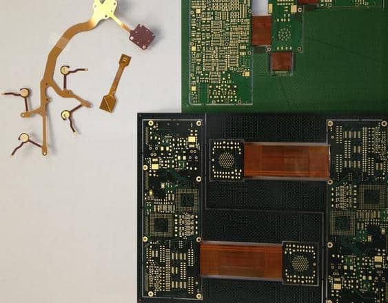
HDI Technology and Microvias
HDI technology has become a cornerstone of modern microelectronics, enabling designers to support increasingly dense component layouts. Microvias allow signals to be routed within highly compact board designs while supporting advanced packages that cannot be accommodated using traditional through-hole approaches.
Implementing microvias requires thinner dielectric materials, finer trace geometries, and specialized fabrication methods. These capabilities enable tighter component placement, greater routing flexibility, and increased circuit density.
Sequential Lamination for Advanced PCB Structures
Many HDI designs require multiple lamination cycles and precision laser drilling to create stacked microvia structures. Sequential lamination allows manufacturers to build complex multilayer PCBs that support demanding routing requirements while preserving signal integrity.
Although these processes increase manufacturing complexity, they are often necessary for producing today’s high-performance electronic products. Close collaboration between PCB designers and fabrication partners helps ensure successful implementation of HDI technologies.
For more information about the evolution of microelectronics and PCB production, visit the San Francisco Circuits website.